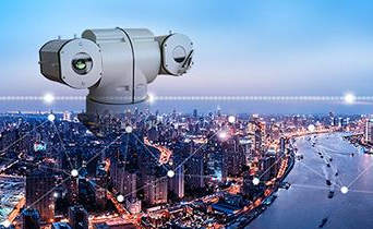
According to a report by Mymes Consulting, a research group project led by an electrical engineer from the University of California, San Diego recently introduced a thin sensor that converts infrared light into visible light images. Tests show that the image sensor can be applied to: (1) Observe the environment through smoke; (2) See through the silicon chip to check the quality and composition of the electronic chip; (3) Monitor the heart rate while drawing images of human blood vessels without touching Subject's skin.

Shortwave infrared image sensor developed by the University of California, San Diego
The image sensor can detect the short-wave infrared part of the spectrum. In practical applications, the imaging system first irradiates short-wave infrared light on the object or area of interest, and then converts the low-energy short-wave infrared light reflected back to the system into visible light with shorter wavelengths and higher energy that human eyes can see .
The short-wave infrared image sensor developed by the research team integrates a photodetector and a display component. A plurality of semiconductor layers are stacked on each other, and the thickness of each semiconductor layer is about several hundred nanometers. Three of the layers are made of different organic polymers: a photodetector layer, an OLED display layer, and an electron blocking layer between the photodetector and the OLED display layer.

Composition and materials of the short-wave infrared image sensor
The photodetector layer absorbs short-wave infrared light or low-energy photons, and then generates a current due to the photoelectric effect, and then flows to the OLED display layer-the current is converted into a visible light image. The electronic blocking layer is used to prevent the OLED display layer from losing any current during the Upconversion process. This allows the sensor to produce clearer images.
Note: Photon Upconversion (Photon Upconversion) refers to the process of absorbing two or more photons with a longer wavelength to excite photons with a shorter wavelength. It is anti-Stoke type luminescence. An example of this type of luminescence is to convert infrared light into visible light. Materials with this luminescence characteristic are called up-conversion luminescent materials, which usually contain elements in d-zone or f-zone. .
Ning Li, the first author of this research, said: “The advantage of up-conversion is that it can achieve direct conversion of infrared light to visible light in a thin and compact device. In a typical infrared imaging system, you need An array of infrared detectors to collect data, a computer to process the data, and a separate screen to display the data. This is why most existing infrared imaging systems are bulky and expensive."
Because the image sensor is made of organic semiconductors, it is low in price, flexible in use, and can be applied to the biomedical field. Many infrared imaging systems currently in use or previously used are expensive, bulky and complicated; they usually require separate imaging cameras and displays. The infrared detectors in the system are mainly made of inorganic semiconductors, which are expensive and may contain Toxic elements such as arsenic and lead.
Compared with similar sensors using inorganic semiconductors, this new device also provides better imaging resolution, can see a wider short-wave infrared spectrum, and integrates a display size of 2 square centimeters. Because the sensor is manufactured using a thin-film process, it can be scaled up easily and inexpensively to make larger devices.
Another important feature of the image sensor is that it can effectively provide optical readout images and electronic readouts. For example, when a researcher irradiates infrared light on the back of a subject's hand, the image sensor records the subject's heart rate while providing an image of the subject's blood vessels.

The image sensor monitors heart rate while drawing images of human blood vessels
In another demonstration, the researchers placed a photomask with an "EXIT" letter pattern in a small room filled with smoke. They also placed a photomask printed with "UCSD" letter patterns behind the silicon wafer. Experimental demonstrations show that short-wave infrared light can penetrate smoke and silicon chips, so that the image sensor can see the above-mentioned letter patterns.

The image sensor can observe the letter patterns on the photomask through smoke and silicon wafers
The current goal of the researchers at the University of California, San Diego is to improve the efficiency of their devices. This research work was supported by the National Science Foundation and Samsung Advanced Technology Research Institute. Related papers were published in "Advanced Functional Materials" (www.doi.org/10.1002/adfm.202100565).
ADD: Floor 5, Block A, Building 1,
Great Wall Innovation Science Park,
East lake high-tech District, Wuhan, China
Contact Admin: info@zipinfrared.net
Tel: +86-27-81296962
Working time:
Mon-Sat 8:30-17:30
We seek inquiries from bona fide businesses about
ZIP Technology dealers.
If you are interested in selling ZIP Technology's products
we can help you integrate those into your existing product line.
As well as attractive dealer prices, we offer technical
and promotional support.