The content of this article is reproduced from the fourth issue of "Infrared and Laser Engineering" in 2021, and the copyright belongs to the editorial department of "Infrared and Laser Engineering".
Abstract: With the continuous development of infrared devices and imaging technology, various night vision systems demand more and more megapixel mid-wave infrared imaging components. Based on the domestic 15 μm 1280×1024 mid-wave HgCdTe detector, based on the detector and the Dewar's own envelope, it broke through the small size, light weight, and integrated design, and developed a compact dual-FPGA processing platform with megapixels Wave infrared imaging core components, component size 155 mm×95 mm×95mm, mass 1400 g, support SDI, Cameralink interface output; blind element replacement, non-uniform correction, noise reduction, detail enhancement, dynamic range are realized on this platform Real-time image processing algorithms such as compression and local enhancement. For traditional infrared imaging algorithms, a non-uniform correction algorithm based on residuals and an adaptive local enhancement algorithm are proposed to improve the imaging performance of the component. Test results show that: the module can output high-quality and low-noise infrared images with a resolution of 1280×1024 pixels in real time, the noise equivalent temperature difference (NETD) is less than 30mK, and the module meets the working requirements of high temperature 60 ℃ and low temperature −40 ℃ . Improve the processing algorithm, and the final output image is significantly improved.
Keywords: infrared imaging; cooled infrared; FPGA; detector assembly; mid-wave infrared
Introduction
Since the introduction of infrared imaging systems in the United States, more than 60 years of development have passed. It uses the principle of photoelectric conversion and signal processing to detect the intensity of infrared radiation on the surface of the target object, and after obtaining the surface temperature of the detected object, it converts it into an electrical signal and finally outputs it in the form of image information. At present, foreign thermal imaging cameras with 1280 and above pixels are already in the application stage. In domestic infrared system applications, the mainstream of medium-wave devices is still 640×512 resolution, but with the continuous expansion of infrared market demand and detector technology and engineering With the mature development of technology, in military fields such as night vision, reconnaissance, surveillance, missile guidance, there will be more and more demand for large-area detection and high-resolution detectors. The mid-wave 1280×1024 infrared megapixel imaging component will be used in the future. Weapon systems, military reconnaissance, strategic defense, etc. have very large application prospects.
Based on the domestic 15 μm 1280×1024 medium wave HgCdTe infrared imaging detector, this article introduces the performance of the detector, the circuit composition of imaging components and the integrated design of the components; for the information acquisition and processing of the large area array, the dual FPGA image is introduced Processing circuit hardware architecture and design plan; developed a software platform with FPGA as the core according to component application requirements; introduced the infrared image algorithm used by the core components, explained the key module algorithms for non-uniformity correction and local enhancement; finally aimed at infrared The imaging components have been tested for low-noise circuit, NETD, high and low temperature and imaging tests.
1 Infrared detector component design
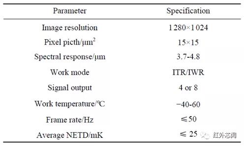
The mid-wave infrared 1280×1024 HgCdTe detector is mainly used to realize the conversion of target infrared signal and electrical signal. A domestic detector is composed of HgCdTe array detector chip, CMOS readout circuit chip, metal Dewar and SCI08R integrated integral Stirling refrigerator. Its performance is shown in Table 1. The pixel center spacing of the detector is 15 μm, the spectral response range is (3.7±0.2)~(4.8±0.2) μm, and the working temperature is 80 K. The detector adopts ion implantation technology in p- A photovoltaic array of 1280×1024 (PV) detectors is made on HgCdTe, which is interconnected with the readout circuit through flip-chip interconnection to realize electrode interconnection to form a hybrid infrared focal plane detector chip set. The readout circuit adopts a 1280×1024 high-performance snapshot mode to read out the integrated circuit. The readout circuit completes the (direct injection) integration, storage, row gating, cell gating, and signal voltage drive output of the photovoltaic diode instantaneous signal. With 1280×1024 window format and window mode, 4 or 8 analog outputs are optional.

Table 1 Detector performance indicators
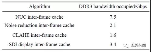
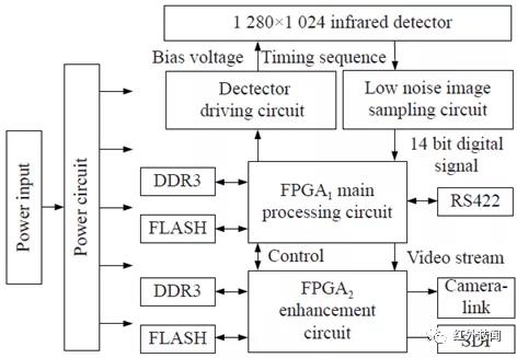
According to the requirements of detector performance and real-time output, the article uses XILINX’s SPARTAN6 as the main processing chip to complete the imaging frame rate of 50 Hz. The circuit imaging part needs to complete the blind element replacement, non-uniformity correction and image enhancement functions. According to the imaging According to the software requirements, the design calculates that the main clock MC is 17.5 MHz, and the pixel clock is 70 MHz, which can meet the requirements of large-area infrared image acquisition, processing and display with a frame frequency of 50 Hz. In this way, the DDR3 bandwidth required for algorithm processing is 14.6 Gbps. Considering that the DDR3 bandwidth of each SPARTAN6 FPGA supports up to 10 Gbps, the dual FPGA architecture is selected in this article to meet the system’s demand for DDR3 bandwidth. In addition, the dual FPGA architecture can Reduce the pressure of FPGA placement and routing, improve the reliability of the program, and reserve resources to support subsequent higher frame rate designs and image processing algorithm upgrades. The specific required bandwidth is shown in Table 2.

Table 2 DDR3 bandwidth required by the algorithm
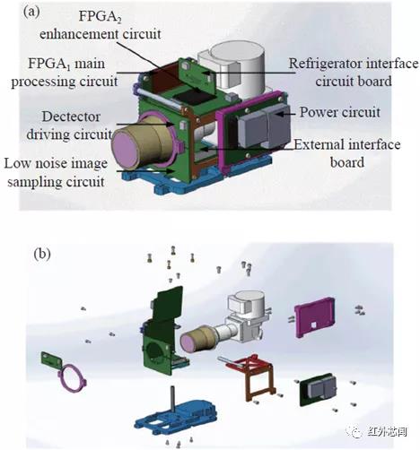
Since the development of the current infrared system has taken into account various needs, the system has been miniaturized and lightened. Therefore, the design concept in the article is to design the components around the outer envelope size of the detector 154 mm×78 mm×57 mm, thereby reducing Component size. As shown in Figure 1: The entire assembly is designed with a lightweight skeleton centered on the detector, which is used to install the assembly system circuit. The system circuit is composed of acquisition circuit, detector drive circuit board, FPGA1 main processing board, FPGA2 enhanced processing board, power supply circuit board, refrigerator interface circuit, and external interface circuit. The refrigerator interface board provides a power filter circuit for the refrigerator. After the refrigerator is cooled to a cooling temperature of 80 K; the infrared focal plane detector performs normal work and starts the photoelectric signal conversion; the dual FPGA image processing circuit drives and controls the detector to perform Image acquisition, processing, and finally output of the processed infrared imaging signal; the power board mainly completes the power supply of the entire circuit system and the detector; the main processing board is designed with a heat sink for component heat dissipation and fixation of the main circuit board. The disassembly of the component structure is shown in Figure 1(b). Its overall size is 155 mm×95 mm×95 mm, which is slightly larger than the outer envelope of the detector, and its mass is about 1400 g.

Figure 1 15 μm 1280×1024 cooling infrared imaging module composition diagram. (a) Schematic diagram; (b) Exploded diagram

Figure 2 Image processing circuit hardware design diagram
So far, we ZIP Technology provides MWIR cooled thermal imaging core with 15um pixel size and 640*512 or 320*256 resolution. Click here to see details.