The invention of the photonic chip has gradually improved the ability of silicon waveguides to carry data. Accordingly, scientists hope to increase the bandwidth of the optical signal transmitted therein. However, for the manufacture of chip-level equipment, multiplexing near-infrared and mid-infrared signals in the same waveguide is a difficult problem to solve.
Today, researchers from Vanderbilt University in the United States have demonstrated a new type of hybrid waveguide that can transmit mid-infrared (wavelength 6.5 μm~7.0 μm) and near-infrared (wavelength 1.55 μm) light waves at the same time. The research was published in the journal Advanced Materials , and the link to the paper is: https://onlinelibrary.wiley.com/doi/10.1002/adma.202004305. This waveguide is made of two different semiconductors and is expected to become a key component of the future integrated photonic structure, which can handle data such as remote communication and chemical spectroscopy.

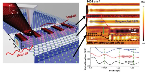
Figure 1 Researchers have designed a hybrid silicon-based photonic waveguide that can transmit mid-infrared and near-infrared light simultaneously on the same chip
Stack of silicon and boron nitride
The hybrid waveguide is made by Vanderbilt University in the United States and is composed of hexagonal boron nitride (hBN) heterostructure and silicon. Joshua D. Caldwell, a professor of engineering at Vanderbilt University, said that the heterostructure is "a structure formed by stacking two different materials together." In the hybrid waveguide they developed, the two materials are silicon and nitride. Boron; Among them, boron nitride exists in the most stable form of a hexagonal lattice similar to graphite.
Scientists have been able to transmit near-infrared frequencies in silicon waveguides, but if they want to transmit mid-infrared waves in them, the size of the waveguide must be larger. The problem is that when the size of the waveguide is large enough to receive mid-infrared signals, the near-infrared transmission will be disrupted.
The hBN material transmits mid-infrared waves in the form of hyperbolic phonon polarization excimers. Researchers at Vanderbilt University in the United States first mathematically modeled, and then fabricated hybrid waveguides through experiments: the waveguide was first etched onto a 220 nm thick silicon wafer, and then a 40 nm thick hBN layer was transferred on it. The research team analyzed the signal pattern passing through the heterostructure with the help of scanning near-field optical microscope.
Future possibilities
Caldwell said that this heterogeneous structure has many potential uses, and explained: "On the one hand, you can use the mid-infrared channel for chemical sensing,'notify' the occurrence of the near-infrared channel detection event, and send the signal to the signal Reading end. In addition, modulating the mid-infrared channel can change the local environment of the underlying silicon channel, thereby providing a means to actively modulate the near-infrared signal. Finally, this waveguide can also be simply used to transmit the same form of two Different kinds of information."
Caldwell said that next he and his colleagues will focus on studying how to integrate these hybrid heterostructures into functional silicon photonic structures, such as ring resonators and photonic crystals, and explore whether these structures can achieve near-infrared and mid-range. Infrared multiplexing.
There are also researchers from three other US institutions participating in this research, from the University of Iowa, Columbia University, and Kansas State University.